User:HLandau/Block Diagram Discussion
< User:HLandau
Jump to navigation
Jump to search
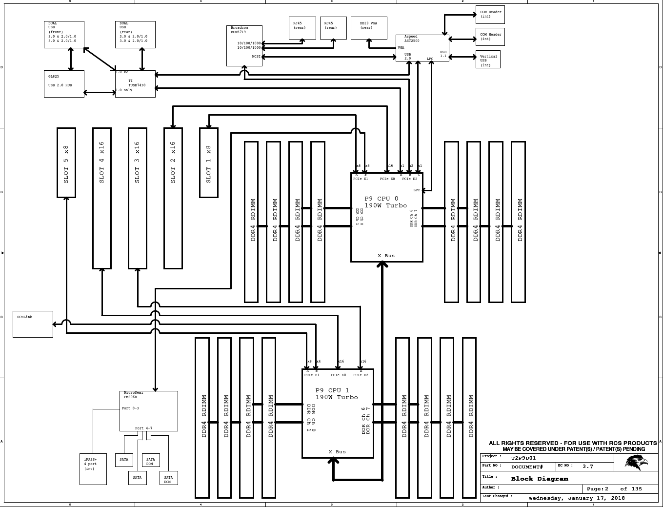
Revision as of 21:38, 8 August 2018 by HLandau (talk | contribs) (Created page with "File:Talos ii rev 3 7 block diagram.png This lists various minor CPU interfaces not shown on the block diagram. For more information about CPU pins, see File:POWER9_Sfo...")
This lists various minor CPU interfaces not shown on the block diagram. For more information about CPU pins, see File:POWER9 Sforza DS v16 23JUL2018 pub.pdf.
Major CPU Interfaces
- X-bus
- Links the two CPUs together. Used for cross-CPU memory access.
- CPU0/1 PCIe E0, E1A, E1B, E2A, E2B, E2C
- Connects various I/O devices and PCIe slots. Includes a PCIe connection to the BMC.
Minor CPU Interfaces
- CPU0 LPC [to FlexVer] to BMC, LPC TPM
- The LPC interface of CPU0 is connected to the BMC. The BMC serves the PNOR flash chip connected to it to CPU0, and CPU0 loads boot firmware from it. A TPM connector is also provided on the board which exposes this bus, and allows a standard TPM to be attached to it.
A FlexVer module, if fitted, can intermediate this bus and proxy all communications between the CPU and other devices on the LPC bus. This switching is done automatically via analogue components on the mainboard when a FlexVer device is connected.
- CPU0 FSI to BMC
- CPU0's front port. This is an IBM-specific slave interface on CPU0 allowing operation of CPU0 to be controlled. It is connected to the BMC, which uses it to tell CPU0 to start. It is also used to retrieve thermal status information via the OCC so that the BMC can set correct fan speeds. When secure boot is disabled, it can also be used as a hardware debugging interface, and is actually the interface used by IBM's own hardware debugging equipment. The program "pdbg", available at the OpenBMC shell, can alternatively be used (e.g. for kernel debugging); thus every mainboard has a hardware debugging environment built into it.
- CPU1 FSI to N/A
- CPU1's front port is not connected, as it is the slave CPU.
- CPU0-CPU1 FSI
- An additional FSI interface provides a master-slave connection between CPU0 and CPU1.
- CPU0/1 AVSBus
- AVSBus, a variant of PMBus, is used to constantly communicate currently desired voltage levels to CPU voltage regulators. The OCC auxillary processor on the CPU controls this interface. Connected to voltage regulators.
- CPU0/1 I2C to DIMM SPDs
- DIMMs contain a small I2C flash chip (SPD chip) containing essential information about the type of DIMM used. Each CPU has I2C interfaces used to connect to these, used as part of DRAM initialization. Connected to DIMM slots.
- CPU0/1 APSS
- Optional SPI interface used for voltage control. Not used in favour of AVSBus. Not connected.
- CPU0 I2C to Planar VPD
- Connects to a small I2C flash chip on the mainboard, the Planar VPD, containing serial numbers and DRAM calibration data for the mainboard (???). This data is needed as part of the boot process. (This can also be used to attach a TPM instead of LPC, but this is not used on the Talos II.)
- CPU1 I2C to Planar VPD
- Not connected, only the master CPU needs this connected.
- CPU0/1 Spare I2C
- Spare I2C for PCIe hotplug use. Not used or connected.
- BMC I2C TO CPU0/1 SEEPROM1
- The SEEPROM on each CPU module contains the SBE boot firmware used for early hardware initialization. The BMC is connected to the I2C lines used to initially program this SEEPROM on both CPUs, and can thus reflash it if it becomes bricked. Read-only when secure mode is enabled.
- BMC I2C TO I2C TPM
- Runs to the TPM connector. Allows connection of a TPM via I2C instead of LPC. In this case, the connection is via the BMC.
- CPU0 JTAG
- Debugging interface available in addition to the FSI front port. Runs to a header on the mainboard.
- CPU0/1 Spare GPIOs
- Three spare GPIOs. Not used or connected.
- CPU0/1 OCC Alert Pin
- Input GPIO which can be used by mainboard to request power throttling.
- CPU0/1 TPM Reset, Interrupt Pins
- Pin used by CPU0 to reset TPM; pin used by TPM to interrupt CPU0. Not used for CPU1.
- CPU0/1 Characterisation Connector
- ???
- CPU0/1 SEEPROM0, SEEPROM3 I2C
- ???
- CPU0/1 Secure Mode Select
- Controlled by jumpers on mainboard. Indicates whether secure boot should be enabled. Can be forced on by a FlexVer module, if fitted.
BMC to Other Interfaces
- I2C link to each PCIe slot.
- I2C links to characterisation connectors.
- I2C link to clock generator.
- I2C link to CPU voltage regulators.
- I2C link to RTC; a connected I2C TPM module, if used instead of an LPC TPM module.
- I2C link to the FPGA; the fan control chip; power supply (PMBus header); temperature sensors.
- SPI link to BMC flash, PNOR flash chips.
- Internal USB1 connector, forwarded to host.
- VGA output, forwarded to host.
- Two serial connectors, one external (RS232), one internal (TTL).
FPGA to ...
- Connected to enable lines for voltage regulators, ATX PGOOD, etc. Handles power sequencing.
